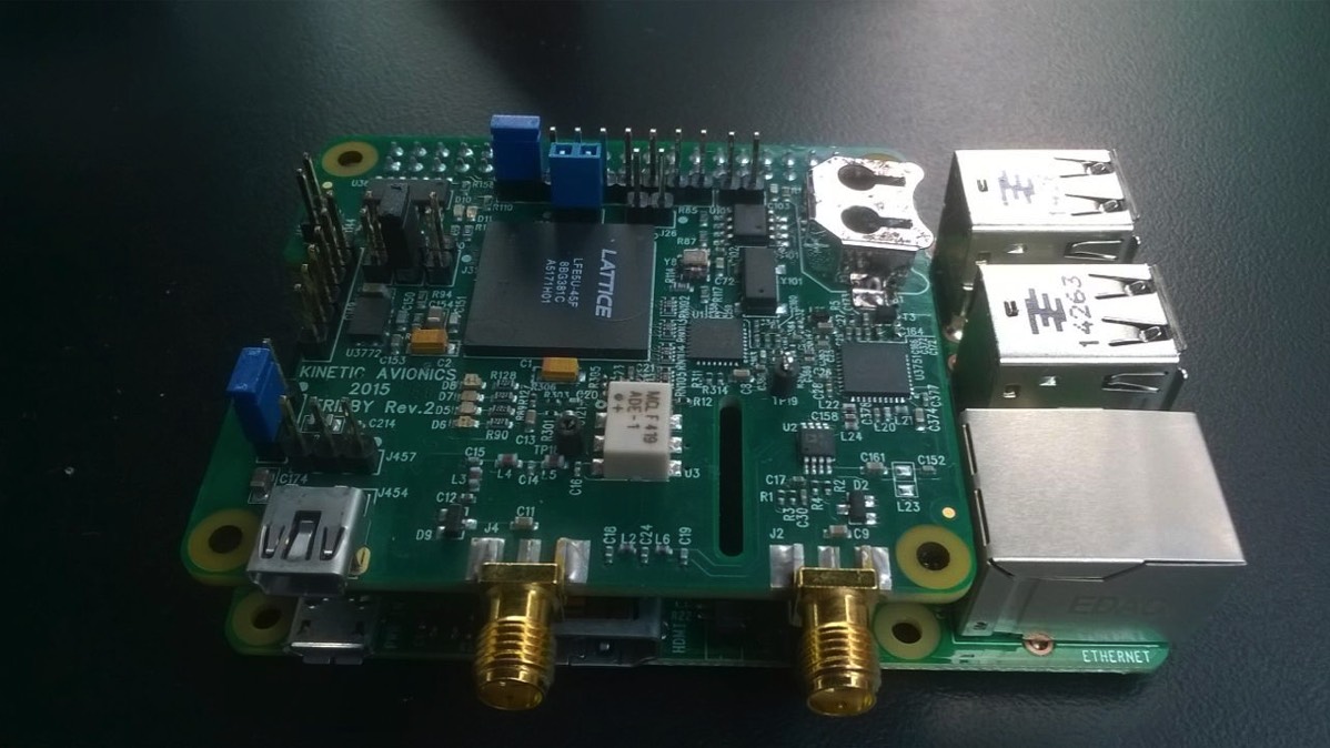
The TRILBY HAT is here !
A revolution in Raspberry Pi HAT functionality & pricing.
What is an FPGA
A Field Programmable Gate Array (FPGA) is an integrated circuit device which can be reconfigured by by the user after manufacturing. It consists of a number of logic blocks which can be configured for different functions
Whats in the FPGA
The FPGA on the Trilby HAT is a member of the Lattice ECP5 family (Part number LFE5U-45)
It has:
It has:
- 21,924 configurable logic slices
- 108 18Kbit memory blocks, giving 1944 Kbits of embedded memory
- Up to 194 Kbits of distributed RAM
- 72 18x18 bit multipliers
- 4 PLL's
What can I do with an FPGA
You can design your own circuits to upload to the FPGA using Lattice Diamond software,
utilising logic components ranging from simple AND and OR gates, flip flops and registers to RAMs, ROMs, multipliers and digital signal processing components.
The device is so large that you can even embed your own microprocessor within your design
Design your circuit on a PC (Windows 7 or 8 required) using Lattice Diamond’s schematic editor, and/or write in a Hardware Description Language: VHDL or Verilog. These languages look similar to a programming language, but you are actually specifying hardware which can allow very fast, parallel operations
Then upload to Trilby HAT using a standard USB cable, a Lattice programming cable or via the Raspberry Pi.
Hardware designs can be uploaded dynamically during operation, or stored in Flash ROM so that it is run on power-up
What could I do with the Trilby HAT
Your design can communicate with the Raspberry Pi using SPI, I2C etc.
It can also control the tuner chip and 4 LED’s on the Trilby HAT board
External circuitry can be attached using the 24-pin I/O expansion connector
Possible applications include:
It can also control the tuner chip and 4 LED’s on the Trilby HAT board
External circuitry can be attached using the 24-pin I/O expansion connector
Possible applications include:
- Learning / experimenting with circuit design
- Designing custom hardware for driving your own circuits
- Prototyping of hardware
- Software Defined Radio
- Digital signal processing
- Image processing and computer vision
- Speech recognition
- Robotics
- Cryptography
- Computer hardware emulation
- Co processors / accelerators to speed up operations such as maths, graphics, encryption
Mission


150kHz to 1000MHz+
Software Defined Radio
Software Defined Radio

HF Up Converter

Real Time Clock

Dual Audio Output Channels / Stereo Capable

4 Coloured LEDs

GPIO FPGA Breakout Connector

Lattice ECP5-45 FPGA

Use Standalone or with Raspberry Pi
Our mission is to be the pre-eminent designer and developer of Avionic, Marine and Software Defined Radio solutions for surveillance monitoring, recording and analysis.

